DLVA's Solid State Components - Application Note
THEORETICAL BACKGROUND - LOG AMPLIFIER DESIGN
I. INTRODUCTION
The limiting factor in processing a wide instantaneous dynamic range signal is the dynamic range of the processing circuitry. Logarithmic amplification solves this problem by transforming a large input dynamic range that increases logarithmically to a small output dynamic range which increases linearly. Since the compression ratio is known, the input signal amplitude information is preserved.
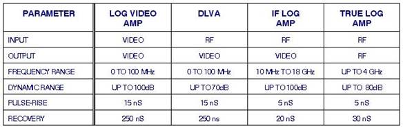
There are several types of logarithmic amplifiers presently available. These include logarithmic video amplifiers, detector logarithmic video amplifiers, logarithmic IF amplifiers, and true logarithmic amplifiers. Each type has its own unique properties. The comparison in Table I shows the key differences in specifications.
II. LOGARITHMIC VIDEO AMPLIFIER
 A Log Video Amplifier (LVA) is a nonlinear video amplifier having the transfer characteristics shown in Figure 1.
This Transfer Function is of the form of: V out = A*log (V in) + Vo A = slope of the log video amp (mV/dBV) Vin = input video signal (volts) Vo = zero signal offset voltage (volts)
The above devices may be further distinguished as AC or DC coupled, "pulse on pulse," and dual (or extended range) types. Within the pulse on pulse category, there can be unipolar and bipolar devices. Often there are "accessory" functions included with the device design and packaging. These extra electrical functions may include threshold circuits, BITE circuits, and AGC or "null loop" functions.
A. AC Coupled Designs (earlier design techniques)
Historically, the most popular devices are the AC coupled ones. "AC" coupling means simply that there are one or more capacitors in series with the signal path through the device and thus DC inputs (or detected CW inputs) cannot be processed. AC coupled devices are the simplest structures and are often adequate performers since individual radar pulses are usually only a few microseconds in duration and of relatively low duty cycle. Such amplifiers can be designed with more than one circuit approach. The design technique used is shown in Figure 2.
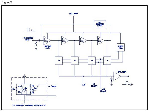
In operation, a detected radar pulse is the input to a serial chain of pulse amplifier stages. These amplifier stages are fast, low power feedback amplifiers. Each stage is designed to smoothly limit at a specific signal level so that, for input signals increasing over the dynamic range, the fourth stage will limit first, then the third, and so on.
While there are other approaches to the realization of a log transfer characteristic, this exclusive approach is highly advantageous because it does not rely on precise semiconductor junction behavior for either transfer accuracy or stability. The "segments" are constructed at relatively high signal voltage levels and gains such that the break points are all easily set with resistor ratios. The involved resistors and reference voltages are all very stable, and volume production of a precisely performing product is readily attainable.
B. DC Coupled Designs (PMI techniques)
 DC coupled designs are used when the amplifier input and output frequency responses needs to extend down to DC to process DC input signals or high duty cycle pulsed inputs. DC coupling eliminates the pulse droop seen on AC coupled LVAs caused by large pulse widths and base line variation caused by high duty cycles.
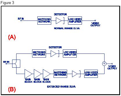
A basic block diagram is shown in Figure 3. This LVA is composed of a cascade of video amplifiers with one or more differential pairs off of the output of each amplifier. The video amplifiers provide high temperature stable, extremely low noise, video gain. This amplified video signal is then the input to the differential pairs. The differential pairs act as transconductance amplifiers. The outputs of all differential pairs are summed together on a "sum" line then transformed into a voltage and video amplified.
DC coupling adds considerable complexity to the design due to the extremely high Dc gain present at low input signal levels (gains can be greater than 1000). Temperature stability becomes difficult, though not impossible, to obtain due to this high gain.
III. DETECTOR LOGARITHMIC VIDEO AMPLIFIER
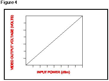
A detector logarithmic video amplifier (DLVA) is an amplifier that has input to output characteristics as described in Figure 4. For an input signal varying over many decades, the resultant output is a linear change over a much narrower range. The ratio between the input dynamic range and the output dynamic range is the compression ratio.
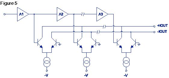
 A block diagram of a DLVA is represented in Figure 5. A DLVA is a detector followed by a logarithmic video amplifier. The detector can be either a Schottky barrier diode or a zero bias tunnel diode. A Schottky diode requires bias and complex temperature compensation circuitry. The tunnel diode, on the other hand, is used in a zero bias configuration (biasing a tunnel diode might improve TSS by 2 dB). The temperature stability of a tunnel diode is much better than a Schottky diode while keeping a reasonable conversion factor, though not as high as the Schottky diode. The type of detector used is determined by the design of the LVA input stage. The Schottky diode requires a high LVA input impedance, and the tunnel diode requires a very low input impedance in order to control the input VSWR.
In basic operation the signal of pulse or CW is detected. The resultant video signal is fed into the LVA and amplified logarithmically. The LVA must have the ability to compensate for the diode non-linearities at high input power levels where the detector is moving from square law operation to linear operation and then into saturation. Also, any temperature related offsets and conversion factor variations caused by detector must be compensated by the LVA.
There are a few important design rules that must be followed in order to achieve the best performance from DLVA design.
A. Dynamic Range
The dynamic range of the DLVA is limited by the dynamic range of the LVA, the TSS level, and the magnitude and linearity of the conversion factor of the detector diode. The lower limit of the dynamic range is determined by the TSS and conversion factor of the detector, and by the sensitivity of the LVA. A logarithmically related input/output transfer function will not occur until the detected video signal is within the lower limit of the LVA’s logging range.
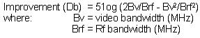
The TSS of the detector is a function of diode type, bias, and RF and video bandwidths. For a given diode, the TSS can be calculated as TSS per 2 MHz + 10log (Bv/2). The diode is connected to the LVA such that the effective noise bandwidth improves the TSS level. This improvement can be calculated as follows:
The new TSS level is now the diode TSS level minus the improvement. The start logging level can be calculated from the TSS level, detector conversion factor, and LVA sensitivity.
The maximum input signal level that can be processed is a function of the detector saturation level, detector conversion factor, and the upper input signal limit to the LVA. The upper limit is reached when either
the detector enters the saturation region, or when the detector supplies a video input signal to the LVA, which causes no change in the video output signal.
B. FREQUENCY FLATNESS
The variation of the detector VSWR and conversion factor due to frequency will appear on the output of the DLVA as an error. The worst case error caused by the frequency variation of the detector occurs when the VSWR ripple and conversion factor variations are added to the LVA maximum deviation from a true logarithmic response. LVAs do not exhibit any errors due to RF frequency variations; only the detector determines errors. By improving the input match of the detector, this variation can be minimized, but care must be taken not to degrade the detector sensitivity and pulse response at the same time.
C. TEMPERATURE EFFECTS
Most DLVAs are required to operate over large temperature ranges and, as such, any errors due to temperature effects must be minimized. Temperature variations will have an effect on the detector conversion factor, noise floor, and on the gain of the video amplifiers. DC offset caused by these variations will be present in the output of a DC coupled DLVA. The temperature effects on a DC coupled DLVA are the most complicated to overcome due to the very high linear video gain associated with signals close to the start logging area in the LVA. With this high gain, any movement in the detector, or any DC offset shift in the first linear video amplifier due to temperature change, will be translated as a huge DC offset in the log output. Attention must be given in the design to achieve a large degree of temperature stability. The use of tunnel diode detectors is an easy way of achieving good detector temperature stability.
D. LINEARITY
Linearity of a DLVA can be explained as the deviation of the actual transfer function of a given DLVA from theoretical value of the logarithmic ratio. A noticeable linearity problem is the point at which the detector is moving from square law operation to linear and then to compression. This effect usually starts at the level of -20 to -10 dBm. To compensate for this effect, an additional logging stage is added in parallel at this point to increase the output onto the sum line. This effectively adds more gain to the upper logging stages in order to compensate for the compression of the detector conversion factor. This type of compensation is good for about 15 to 20 dB of input level above the detector break point; anything beyond this level must be solved in a more complicated detector design.
E. VSWR
The input VSWR of a DLVA is determined by the match of the detector diode. The VSWR of the detector is worse at the transition point from square law to linear region. One way of improving this is by using the detector as a current source. This is done by connecting the detector into a virtual ground on the first linear video amplifier in the LVA (tunnel diode). Another way is to build a matching network at the input of the detector. This type of solution will result in loss of sensitivity and more restricted frequency bandwidth of the input RF signal.
F. EXTENDED DYNAMIC RANGE
The lower end of the dynamic range of a DLVA is determined by the minimum detected signal at the detector. A common value for TSS of a Schottky detector is around -50 dBm per MHz. This value is then modified by the RF and video bandwidths. In some applications, where a wider dynamic range is required, the lowest input signal level will be below the minimum detected signal. Then RF gain must be introduced to the system. Because the dynamic range of the DLVA and the detector is limited, the system will have to be built out of a number of LVAs and detectors. In this configuration, the signal has two paths: one is through the RF amplifier and DLVA 1, and at the saturation point of DLVA 1 the signal is processed through DLVA 2. The summation of the two video signals will give an extended range DLVA.
Careful attention should be given to the temperature, frequency, and gain performance of the RF amplifier since that will affect the overall linearity performance. Another possible error is the level at which the output switches between DLVA 1 and DLVA 2. This error is controlled by the same manner the detector saturation error is handled.
The frequency response of a DLVA is solely determined by the detector that is capable of multi-octave high frequency responses.
Depending on the application, the DLVA can be AC or DC coupled. The DC coupled DLVA is required, operating up to and including CW or in a system with very high duty cycle pulses.
Recent advances in the design of RF amplifiers opened the way to a more realizable IF successive detection approach that has a much superior pulse performance and, at the same time, supplies a limited RF output. Though these advances are being made, the DLVA is still the most convenient approach for extra wide bandwidths (multi-octave), and for frequency bands above 10GHz, it is practically the only economical realizable approach.
