Glossary of Terms and Definitions
DEFINITIONS AND A GLOSSARY OF TERMS FOR DETECTOR LOGARITHMIC VIDEO AMPLIFIERS AND RELATED PRODUCTS
1. INTRODUCTION:
To deal with signals that have high density pulses with narrow pulse widths and large amplitude variations it is often necessary to utilize Logarithmic Amplifiers. Logarithmic (Log) Amplifiers (Amps) compress a large input dynamic range into smaller more usable dynamic ranges through the use of a logarithmic transfer function.
The transfer function causes the output voltage variation (swing) of the log amp to be proportional to the input signal power range in dB. Mathematically speaking, a log amp produces an output voltage that is proportional to the logarithm of the input voltage or input power in dBm. Therefore, a logarithmic amplifier effectively compresses the large input range of the amplifier and can handle a signal amplitude range that would saturate an ordinary amplifier. Because the log amp compresses the amplitude range in a manner that is accurately known, the information about the amplitude of the signal is retained.
There are three types of logarithmic amplifiers: the Detector Log Video Amplifier (DLVA), the Successive Detection Log Video Amplifier (SDLVA or SDLA) and the True Log Amplifier (TLA).
2. DETECTOR LOG VIDEO AMPLIFIER (DLVA):
The Detector Log Video Amplifier or DLVA can deal with the widest range of input frequency. In these devices the RF detection takes place before the logging action. The output of the detector is then compressed to simulate a logarithmic input/output relationship in the log amplifier section which follows.
The dynamic range of a DLVA is limited by the linear/square law range of the input diode detector. The typical dynamic range for a DLVA is in the order of 40 dB. The overall dynamic range of the DLVA can be extended by using two parallel detectors circuits, one with an RF preamplifier. These ERDLVA’s can have dynamic ranges exceeding 70 dB.
The DLVA is usually found in applications in which the original RF frequency is applied directly to the amplifier without the need for down- conversion. Examples of these applications are phased-array radars and direction-finding receivers or channelized receivers.
DLVA circuits are further classified as DC-Coupled, AC-Coupled and Pseudo-DC-Coupled. This terminology refers to the circuitry of the log amplifier that comes after the detector.
DC coupling is used in a DLVA when it is necessary for the circuit to respond to CW signals by producing a continuous DC output that is proportional to the CW input level. Such a design is very complex because of the compensation that is required for drift in the amplifying circuitry.
AC coupling or Pseudo-DC coupling can be used in the video stages of a DLVA when CW response is not required or is not desirable. It is important to note that Pseudo-DC coupling may not be preferable to temperature compensated true DC-Coupled devices.
3. SUCCESSIVE DETECTION LOG VIDEO AMPLIFIER (SDLVA):
The Successive Detection Log Amplifier (SDLA) and the Successive Detection Log Video Amplifier (SDLVA) use circuitry that does not require detection before the logging process. Similar to the DLVA, the SDLA and SDLVA preserve the amplitude information. They both use multiple compressive stages of RF gain to emulate the exponential transfer function. The output of each stage is coupled into a linear detector. The typical dynamic range of each amplifier/detector stage is approximately 10dB, therefore, many such stages are required to cover a large dynamic range. The outputs of each detector stage are then summed in a single video amplifier so as to provide a single detected output. SDLVAs and SDLAs can produce a limited RF/IF output from a separate port. This output is an amplified and limited replica of the input signal.
SDLVAs and SDLAs can also provide very fast rise and settling times because the signal gain and compression takes place in RF circuitry.
SDLVAs and SDLAs are often used in radar missile homing systems, radar altimeters and to drive phase detectors or frequency discriminators.
4. TRUE LOG AMPLIFIER (TLA):
The TLA is different from the other two types of Log Amps in that it does not provide an envelope detected output. The output signal is actually an RF signal compressed in dynamic range by a logarithmic scale. Like both the DLVA and the SDLVA/SDLA, the output signal’s voltage is proportional to the input signal power in dB. The TLA output retains both the amplitude and the phase information for signal processing. These units are usually used in applications where sound is involved, such as sonar, IFF and navigation systems.
5. ABSOLUTE ACCURACY:
The Absolute Accuracy is a measure of the total power uncertainty around a fixed mathematical straight line (reference line) as the RF frequency, RF power and temperature is varied. Absolute Accuracy includes the effects of the log linearity, frequency, output DC offset variation and the temperature variation. It is measured in dB.
6. AMPLIFIER BANDWIDTH:
The Amplifier Bandwidth includes the operational bandwidth and any additional frequency range necessary to accommodate the pulse width and rise and fall times.
7. CW IMMUNITY DYNAMIC RANGE:
This defines, in dBm, the range over which a CW signal will be rejected so as not to affect the pulse performance beyond specifications. It determines the threshold sensitivity value for pulses in a CW environment.
8. CW REJECTION TIME:
The CW Rejection Time is the time required by the device to cancel the maximum specified CW level so that the pulse level at the threshold sensitivity value can be measured within a specified error value. The rejection time can be different when the CW turns "on" and when it turns "off".
9. DYNAMIC RANGE:
The Dynamic Range is the range of the input signals in dB over which the output linearity requirement is met. It can also be defined as the range, as measured in dB, from the TSS to the end of the logging range.
10. DC OUTPUT OFFSET:
The DC Output Offset is defined as the output DC voltage with no RF signal applied and the input RF port terminated into 50 ohms.
11. DC OUTPUT OFFSET VARIATION:
The DC Output Offset Variation is the output voltage variation without any RF signal applied and as the temperature is varied over the operating range.
12. DWELL TIME:
Dwell time is defined as the minimum time for the output pulse to be "Flat" within a specific dB range for the test condition or the minimum required pulse width. It is typically equal to the pulse width less the settling time and is sometimes known as "Flat Top".
13. DROOP:
The output of an AC-Coupled or Pseudo-DC Coupled DLVA will usually return to its initial value, even though an input signal continues to be applied. This is called Droop and it is measured as a percent for a given pulse width.
14. FALL TIME:
Fall Time is defined as the time difference between the 90% and the 10% points on the trailing edge of the output video pulse.
15. FREQUENCY FLATNESS:
The Frequency Flatness is the output voltage variation at a constant temperature and constant RF input power as the RF frequency is varied. It is measured in dB.
16. GAIN FLATNESS vs. FREQUENCY:
The output of a log amp should remain constant in spite of variations in the input frequency. In the DLVA the frequency dispersion is a function of the detector and very wide frequency ranges can be obtained with fairly flat signal gain. Gain flatness can also be a function of the input RF power level used when testing the DLVA. For critical applications it may sometimes be desirable to test gain flatness at room temperature and also at the maximum and minimum temperature extremes, producing curves over the entire power level range in 10 dB increments.
17. INCREMENTAL LOG SLOPE:
The Incremental Log Slope is defined a the slope of the "Best Fit Straight Line" or slope of a defined fixed slope straight line which passes through the actual output voltage data over a limited logging dynamic range.
18. INPUT DYNAMIC RANGE:
The Input Dynamic Range is the range of the input signal over which the logging accuracy is satisfied.
19. INPUT FREQUENCY RANGE:
The Input Frequency Range is the range of the input signal frequency over which the required electrical parameters are met.
20. INPUT SWR:
The Input SWR (Standing Wave Ratio) characterizes how well the input of the log amplifier matches the impedance of the system, usually 50 ohms.
21. LOGGING ACCURACY:
Logging Accuracy is the absolute accuracy with which the output voltage represents the input power. The Log Accuracy is typically specified over the operating temperature range and the input frequency. It defines the worse case deviation of the logging curve from a "Best Fit Straight Line".
22. LOG SLOPE:
The Log Slope is the change in the output voltage per the change in the input power. It is usually measured in millivolts per dB. The Output Slope is normally taken as the slope of a "Best Fit Straight Line" passing through points measured over the entire transfer curve (logging range). For the greatest accuracy the "Best Fit Straight Line" is calculated using the Linear Regression method.
23. LOG LINEARITY:
The Log Linearity is defined as the deviation between the actual measured output voltage and the corresponding point on a "Best Fit Straight Line" that has been derived from measured data and computed using either the Linear Regression method or the Least Squares method (the Linear Regression method is considered more accurate).
24. MAXIMUM INPUT POWER:
This is the maximum RF power that a log amp can withstand without damage.
25. MINIMUM PULSE WIDTH:
The measurement of the Minimum Pulse Width characterizes the ability of a log amp to respond to short duration pulses. It is defined as the pulse width for which the amplifier response differs by no greater than a specified amount from the response to an optimum (longer) pulse.
26. NOISE FIGURE:
The Noise Figure of any amplifier characterizes its noise power spectral density relative to the input of the device. The Noise Figure is an RF parameter that cannot be measured on a logarithmic amplifier because the gain stages are nearly into saturation from their own noise. The Noise Figure may be measured at the IF limited output of an SDLVA/SDLA and also at the output of a TLA. However, the Noise Figure is not an appropriate measurement at the video output of either a DLVA or an SDLVA/SDLA the TSS is used instead.
27. OPERATIONAL SENSITIVITY:
The Usable or Operational Sensitivity is the equivalent to an 8 dB output Signal to Noise Ratio (SNR). This is approximately 4 dB greater than the equivalent Tangential Signal Sensitivity (TSS).
28. OUT OF BAND REJECTION:
This is defined as the ability of the log amp to reject RF signals that are outside the specified frequency band of interest.
29. OUTPUT LOAD IMPEDANCE:
The Output Load Impedance of a log amp is the typical value of impedance into which the specified electrical parameters are met.
30. OUTPUT RANGE:
This is the range of output voltage that corresponds to the operating input power range of a DLVA or SDLVA/SDLA. Input Dynamic Range, Logging Slope and Output Range are related. Given any two the third can be determined.
31. OUTPUT RMS NOISE LEVEL:
This is the maximum AC noise component permissible in terms of RMS value. It is the noise power as measured at the video output with a true RMS voltmeter.
32. PARTIAL RECOVERY TIME:
The Partial Recovery Time is defined as the time required for the output trailing edge to fall from 1.0 dB below peak to some specified level below peak. Usually the Partial Recovery Time is measured for a 16 dB or 20 dB drop in the output trailing edge voltage. The parameter is most useful when two pulses whose amplitudes are very closely spaced need to be measured.
33. PROPAGATION DELAY:
The Propagation Delay can be defined as the delay from 50% RF input to 50% Video output. It can also be defined as the delay time from 50% RF input to 10% Video output as the compression process changes the rise time as a function of the input RF power level.
34. PULSE ON PULSE:
Also known as Pulse on CW. This describes a requirement in a device whereby the pulse amplitude of a signal riding on a CW or RF noise level can be accurately measured. Typically the pulse level can be either weaker or stronger than a specified CW or noise level and needs to be measured accurately.
35. RECOVERY TIME:
The Recovery Time for a Logarithmic Amplifier is best defined as per each application and requirement. There are several accepted definitions:
- The time from the 90% point of the trailing edge of the first pulse to the 10% point on the leading edge of the next pulse.
- The time from when the trailing edge of the pulse exceeds the settled value by an amount equal to the linearity specification to the time within 1 dB of the specified offset.
- It can also be defined as the length of time required between two pulses before a given degree of accuracy can be obtained in measuring the second pulse.
- It can be stated to be the amount of time for the log amp output to return to within some small percentage of its original value after the input signal is removed.
36. RISE TIME:
The Rise Time is commonly defined as the time required for the leading edge of a video output pulse to change from 10% to 90% of its final value for a specified voltage level of the input pulse (the time difference between the 10% point to the 90% point on the rising leading edge of the output video pulse).
37. SETTLING TIME:
This is defined as the difference between the 10% point on the leading edge of the video pulse to the first point in time where no deviations are outside a specified window of the final steady state value.
38. TANGENTIAL SIGNAL SENSITIVITY (TSS):
The Tangential Signal Sensitivity (TSS) occurs when the peak video voltage is 2.51 times the RMS noise voltage. This corresponds to a signal to noise ratio of 8 dB. TSS is dependent on the video bandwidth, detector figure of merit, and the video amplifier noise performance. TSS is the minimum pulsed signal required to offset the output baseline until it becomes even with or tangential to the output noise peaks. The TSS is directly related to the noise figure and the bandwidth and it assists in the defining of the lower limit of the input dynamic range of a log amp. It defines the input level that results in an output SNR of 6, 7 or 8 dB depending upon the definition used. TSS is a convenient way to specify a log amp’s noise performance because of the difficulty in measuring the noise of a log amp at the detected video output.
TSS Measurement TIPs:
- Set up equipment as shown in Figure 1.
- Set power level at the DUT input to Minimum specification noted in product feature.
- Apply DC power to the DUT.
- Measure the peak signal referred to ground with a Digital Multimeter and record value in mV.
- Turn the RF power off and measure the DC offset with a Digital Multimeter.
- Record the Output Offset Voltage in mV.
- Subtract the DC Output Offset Voltage in step (5) from the peak signal measured in step (4).
- Set up equipment as shown in Figure 2.
- Measure the RMS noise voltage with the Digital Oscilloscope (AC coupled).
- Divide the result of step (7) by the RMS noise measured in step (9). This result is the measured ratio.
- Verify that the minimum ratio is 2.51.
- TSS Results:
- Calculate Measured TSS: TSS (dBm) = Input Power Level used in steps (2 through 4) – 10log(Measured ratio calculated in step (10) / 2.51)
OR
2. Calculate Measured TSS: TSS (dBm) = Input Power Level used in steps (2 through 4) – [1/2*([20*log [ {DC Output peak signal from step (4) - DC Offset from step (5)} / RMS Noise from step (9)] ] - 8 dB)]
Record the result in the summary data sheet.
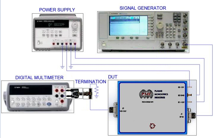
Figure 1
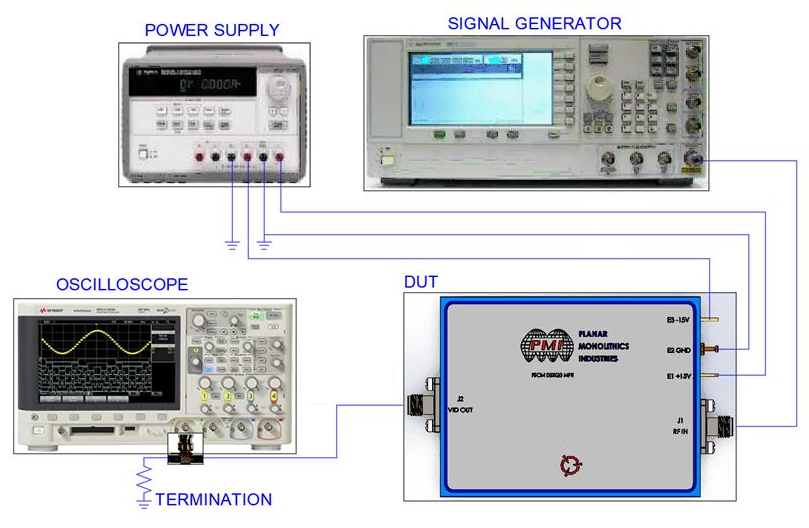
Figure 2
39. THRESHOLD SENSITIVITY:
This is the same definition as Operational Sensitivity.
40. USABLE SENSITIVITY:
This is the same definition as Operational Sensitivity.
41. VIDEO BANDWIDTH:
This is usually defined by either calculations made from accurate rise time measurements or by injecting a swept CW signal into the video section characterizing the output.
