PTRAN-100M18G-SFB-3UVPX-10HP-MAH

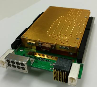
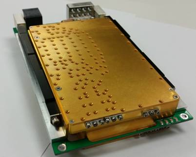
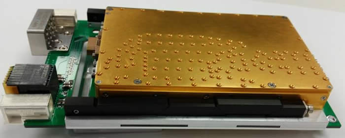
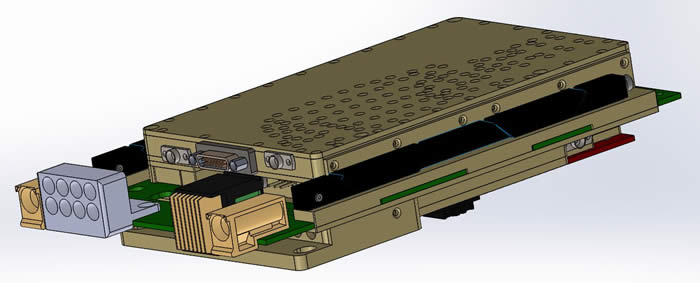
PMI Model PTRAN-100M18G-SFB-3UVPX-10HP-MAH is a transceiver covering the frequency range of 0.1 to 18 GHz. The transceiver fits into a 3U open VPX form factor utilizing the high speed VITA 67 RF connector. This unit up-converts a 0.1 to 4 GHz transmit signal to the 2 to 18 GHz range. It also down-converts a 0.1 to 18 GHz received signal to the 0.1 to 4 GHz intermediate frequency range for analog to digital conversion. A receive filter bank incorporates a 2-way absorptive switch to select an input along with two 6-way switches allowing one of six filter paths to be chosen. A filter bank is used also on the transmit path with two 6-way switches allowing one of six filter paths to be chosen. The unit is made to attach to an FPGA controller card allowing for total solution in a 10HP (2") form factor.
Quick Links: (click the links below for additional information)
Product Feature - PTRAN-100M18G-SFB-3UVPX-10HP-MAH
Transmit/Recieve Filter Bank Information:
Model 6SFB-CC-100M18G-MAH-RX-TX
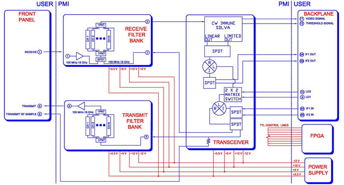
Functional Block Diagram
(Click to Enlarge Image)
Specifications:
| Inputs | J1, J4A, J4B, J9, J10 |
| J1 Input | RF Receive Input |
| Frequency | 0.1 to 18 GHz |
| Power Level | -80 to -10 dBm Typ |
| Connector | SMPM Male |
| J4A Input | IF1 Input |
| Frequency | 0.1 to 4 GHz |
| Power Level | 0 dBm Typ |
| Connector | VITA 67 |
| J4B Input | IF2 Input |
| Frequency | 0.1 to 4 GHz |
| Power Level | 0 dBm Typ |
Connector | VITA 67 |
| J9 Input | LO1 Input |
| Frequency | 4 to 20 GHz |
| Power Level | +10dBm typ |
| Connector | VITA 67 |
| J10 Input | LO2 Input |
| Frequency | 4.0GHz to 20.0GHz |
| Power Level | +10dBm typ |
| Connector | VITA 67 |
| Outputs | J3A, J3B, J6, J8, J11, J12 |
| J3A Output | IF1 Output |
| Frequency | 100MHz to 4.0GHz |
| Power Level | 0dBm typ for limited SDLVA Channel |
| Connector | VITA 67 |
| J3B Output | IF2 Output |
| Frequency | 100MHz to 4.0GHz |
| Power Level | 0dBm typ for limited SDLVA Channel |
| Connector | VITA 67 |
| J6 Output | RF Trasmit Output |
| Frequency | 100MHz to 18.0GHz |
| Power Level | 0dBm to +10dBm typ |
| Connector | SMPM(M) |
| J8 Output | RF Trasmit Sample |
| Frequency | 100MHz to 18.0GHz |
| Power Level | -40dBm to -30dBm typ |
| Connector | SMPM(M) |
| J11 Output | Log Proportional Detected Video Output(V1) |
| Connector | SMA(F)(Cabled to UMC(F)) |
| J12 Output | Threshold Detected Video Output (V0) |
| Connector | Mezzanine Connector |
| Power Supply | Provided by an open VPX backplane through P0 connector rated for the below voltages. |
| +12V | 2 A |
| +5V | 1.5A |
| +3.3V | 0.5 A |
| -12V | 1 A |
| Size | 6.299" x 3.937" x 1.915" (3U Open VPX Card to take up 10HO with FPGA Card) |
| RF Connectors | VITA 67, 8 Position |
| Digital Control | TTL Through Mezzanine Connector ('0':0 - 0.8 Volts), ('1': 2-5 Volts) |
| Finish | Gold Plated |
| Control Logic | TTL ('0'; 0 - 0.8Volts), '1' 2 - 5 Volts) |
| TTL1 | Transmit Path Output Select, Receive Filter Bank Input Select 0 - Output to TX Filter Bank, RX-Backplane/ Input (J1) 1 - Output to RX Filter Bank, RX-Transceiver Input |
| TTL 2 | Receive Filter Select 001 - Channel 1 010 - Channel 2 011 - Channel 3 100 - Channel 4 101 - Channel 5 110 - Not Defined 111 - Not Defined |
| TTL 3 | Linear or Limited SDLVA RF Output Channel 0 - Limited RF Output Channel 1 - Linear RF Output Channel |
| TTL 4 | Receive Thru Channel or Down-Converted Channel 1 - Down-Converted Channel |
| TTL 5 | IF1 or IF2 Output Select 1 - IF2 Output Channel |
| TTL 6 | IF1 or IF2 Input Select 0 - IF1 Input Channel 1 - IF2 Input Channel |
| TTL 7 | Transmit Thru Channel or Up-Converted Channel 0 - Thru Channel 1 - Up-Converted Channel |
| TTL 8 | Transmit Filter Select 000 - Thru Channel 001 - Channel 1 010 - Channel 2 011 - Channel 3 100 - Channel 4 101 - Channel 5 110 - Not Defined 111 - Not Defined |
| TTL 9 | 5 Bit Attenuation Control (1dB Steps) 00000 - 0dB Attenuation 11111 - 31dB Attenuation |
| TTL 10 | LO Select 00 - M1-LO1, M2-LO1 10 - M1-LO2, M2-LO1 11 - M1-LO2, M2-LO2 |
| TTL 11 | SDLVA Threshold Adjust 000000 - Lowest Threshold Level 111111 - Highest Threshold Level |
| TTL12 | SDLVA CTL A (Enable) 0 - Internal Comparator Triggered SPST 1 - External Trigger Enable (SW CTL B) |
| TTL 13 | SDLVA CTL B (Trigger) 0 - Limited RF CH SPST ON (Insertion Loss) |
| Receive Switched Filter Bank | |
| J1 Path Gain | 18dB typ |
| J7 Path Insertion | 10dB typ |
| Isolation | J1, J7 100dB |
| Transmit Switched Filter Bank | |
| Gain | 32dB typ |
| Receive and Transmit Switched Filter Banks | |
| VSWR Over 90% Passband | 2.0:1 max |
| Switching Speed | 100ns typ |
| Thru Channel Passband | 100MHz to 18.0GHz |
| Channel 1 Center Frequency | 3400MHz |
| 3dB Bandwidth | 2000MHz |
| Rejection | -40dBc typ 100MHz - 2.0GHz, -30dBc min -40dBc typ 4.8GHz - 18.0GHz, -30dBc min |
| Channel 2 Center Frequency | 5400MHz |
| 3dB Bandwidth | 2000MHz |
| Rejection | -40dBc typ 100MHz - 4.0GHz, - 30dBc min -40dBc typ 6.8GHz - 18.0GHz, -30dBc min |
| Channel 3 Center Frequency | 7400MHz |
| 3dB Bandwidth | 2000MHz |
| Rejection | -40dBc typ 100MHz - 6.0GHz, -30dBc min -40dBc typ 8.8GHz - 18.0GHz, -30dBc min |
| Channel 4 Center Frequency | 9400MHz |
| 3dB Bandwidth | 2000MHz |
| Rejection | -40dBc typ 100MHz - 8.0GHz, -30dBc min -40dBc typ 10.8GHz - 18.0GHz, -30dBc min |
| Channel 5 Center Frequency | 11400MHz |
| 3dB Bandwidth | 2000MHz |
| Rejection | -40dBc typ 100MHz - 10.0GHz, -30dBc min -40dBc typ 12.8GHz - 18.0GHz, -30dBc min |
| SDLVA | |
| V0(Video Comparator Signal Amplitude) | LVTTL |
| Video Comparator Delay | 50ns typ |
| Video Comparator Threshold Level | Adjustable with analog voltage -60dBm ±3.0dB max |
| V1 (Log Video Signal Amplitude) | 1 Volt max |
| Log Slope | 10mV/dB into a 50Ohm Load (±1 mV) max |
| Log Range | -65 to +5dBm min |
| Log Linearity | ±1.75dB (-40°C to +85°C) max |
| Pulse Range | 100ns to 250us |
| Rise Time | 35ns max |
| Settling Time to ±1dB | 50ns typ |
| Recovery Time | 350ns max |
| CW Immunity Range | TSS to -45dBm (1dB Degradation) |
| Pulse Considered "CW" | 1ms typ |
| Rejection Time | 1ms typ |
| Droop | 1dB max |
| SPST Isolation | 70dB typ |
| SPST Switch Speed | 20ns typ |
| SW CTL A (Enable) | TTL0: Internal Comparator Triggered SPST TTL1: External Trigger Enable (SW CTL B) |
| SW CTL B (Trigger) | TTL 0: Limited RF CH SPST Switch On (Insertion Loss) TTL1: Limited RF CH SPST Switch Off (Isolation) |